Category: Uncategorized

  • Hamamatsu Silicon Photodiode S1787-04 S1787-08 S1787-12

    Hamamatsu Silicon Photodiode S1787-04 S1787-08 S1787-12

    Hamamatsu Photodiode S1787

    S1787-04 Plastic package photodiode with low dark current at hamamatsu company website

    S1787-04 is a family of plastic package photodiodes that offer low dark current. Plastic package used is light-impervious, so no stray light can reach the photosensitive area from the side or backside. This allows reliable optical measurements in the visible to near infrared range, over a wide dynamic range from low light levels to high light levels.

    Datasheet for S1787

    Other sellers,

    Aliexpress S1787-04 Si photodiode Plastic package photodiode with low dark current S1787.

    eBay 1PCS S1787-04 Silicon photodiode, wavelength 560nm 320-730nm for visible light.

    gophotonics The S1787-04 from Hamamatsu Photonics is a Photodiode with Wavelength Range 320 to 730 nm, Capacitance 700 pF, Dark Current 10 pA, Responsivity/Photosensitivity 0.19 to 0.3 A/W, Rise Time 2.5 µs. More details for S1787-04 can be seen below.

  • hamamatsu

    hamamatsu

    Hamamatsu Photonics Products – Official Website Hamamatsu

    Hamamatsu Photonics is a leading company of light technology and products. High level solutions for photometry systems, light sources, cameras, etc. Research projects.

    Hamamatsu Photonics K.K. (浜松ホトニクス株式会社, Hamamatsu Hotonikusu Kabushiki-Kaisha) is a Japanese manufacturer of optical sensors (including photomultiplier tubes), electric light sources, and other optical devices and their applied instruments for scientific, technical and medical use.

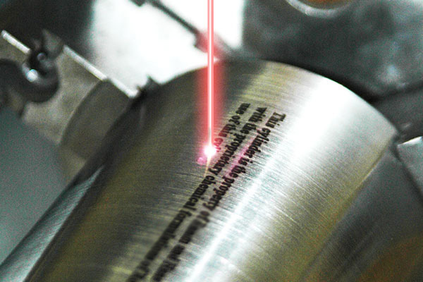
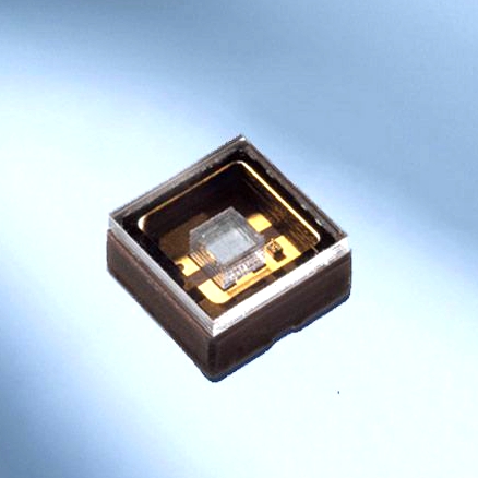
    Hamamatsu Photonics is a leading manufacturer of devices for the generation and measurement of visible, infrared, and ultraviolet light. These devices include photomultipliers, photodiodes, infrared detectors, image sensors, scientific cameras, and light sources. We also offer x-ray detectors and sources, as well as specialized photometric systems for semiconductor manufacturing, pharmaceutical development, nondestructive inspection, and academic research.

    Hamamatsu is dedicated to the betterment of life through light-based technologies. Based on this corporate philosophy, we conduct basic research on the fundamental properties of light, while also making extensive R&D efforts in the development of new products. Our devices are used in scientific, industrial, and commercial applications around the world. We have a global network of operations.

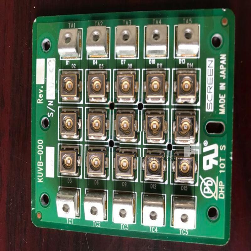
    In Japan: Global headquarters, manufacturing, and research facilities are located in Hamamatsu, Japan. Here we have four primary manufacturing divisions: Electron Tube Division (for products such as photomultiplier tubes, scintillators, light sources, and x-ray sources); Solid State Division (photodiodes, silicon photomultipliers, image sensors, infrared detectors, x-ray detectors, MEMS devices); Systems Division (scientific cameras, photometric systems); and Laser Group (laser diodes, quantum cascade lasers). Tokyo Stock Exchange, TYO: 6965.

    In the Americas: Hamamatsu Corporation is the North American subsidiary of Hamamatsu Photonics. Our headquarters is in Bridgewater, NJ and we have a branch office in San Jose, CA.

    In Europe: Hamamatsu Photonics Europe GmbH is the regional headquarters. Primary sales offices are located in Germany, France, Italy, Sweden, and the United Kingdom. Satellite sales offices in several other countries.

    In Asia: Hamamatsu Photonics (China) Co., Ltd. in Shanghai provides primary sales support in China.

  • 50W 100W Laser Pointers

    50W 100W Laser Pointers

    There are lots of high power laser pointers labelled 50W , even 100W on aliexpress, you can also find many 50W laser pointers online.

    But in fact, the output power of 50W is not the real output power. The most powerful laser pointers is about 5W or 5000mW. They’re not 50W or 50000 mW . Many sellers label a regular 50mW laser pointer to 50W, because many customers like high power lasers.

    Check this 50000mw 520nm Gatling Burning High Power Green Laser pointer kits on laserpointerpro . It’s not 50W laser pointer.

    This 50000mW World’s Strongest Handheld Laser Pointer Ultra Powerful Bright Blue Beam Light Flashlight from htpow . It’s not 50W laser pointer.

  • Laser Marking near me

    Laser Marking near me

    If you need “Laser Marking near me”, you may just need laser marking service nearby. Here we list the address of different laser marking service companies.

  • Where to find Laser Marking Services

    Where to find Laser Marking Services

    We list some companies who can offer Laser Marking Services.

    1. lasermarkingsvs
      12675 Danielson Court, Ste. 402
      Poway, CA, 92064
      P: 858-748-3468
      E: info@lasermarkingsvs.com

    Their laser marking systems are capable of marking a wide range of materials. As a guide, we have listed a number of materials below; however, please be aware that this is not an exhaustive list so please contact us if your material is not listed:

    • Stainless Steel
    • Wood
    • Aluminum
    • Carbide
    • Nickel
    • Titanium
    • Cast Iron
    • Chrome
    • Painted Metal Alloys
    • Multi-Coated Metals
    • Plastics
    • Backlit Buttons
    • Polycarbonate
    • Polypropylene
    • PVC
    • Rubber
    • Composite

  • Laser Marking Services

    Laser Marking Services

    You can find some Laser Marking Services online. Here are some useful advice for you to choose Laser Marking Services.

  • Nichia LED NCSU434A UVC 17mW 280nm 0.5W

    Nichia LED NCSU434A UVC 17mW 280nm 0.5W

    Nichia LED NCSU434A UVC 17mW 280nm 0.5W Japan Original

    High performance UV-C NCSU434A SMD LED with 280nm and 17.5mW typical radiant power
    Typical voltage 5.3V, current 100mA
    Typical power consumption: 0.5W
    120 deg viewing angle
    Dimensions (LxWxH): 3.5×3.5×1.72mm

    Application areas: Disinfection, Sterilization

    Weight (g) 1.000000
    LED Installation Package Emitter
    Color UVC Ultraviolet
    Viewing Angle 120°
    Forward Current Typ 350ma
    Forward Voltage Typ (V) 5.3
    Power (W) 0.5
    Wavelength (nm) 280
    Manufacturer Product Code NCSU434A UV-C

  • NVSU035B 395nm UV 3D printer UV module light source

    NVSU035B 395nm UV 3D printer UV module light source

    3D UV LED printer curing light source module NVSU035B 395nm UV

    Specification

    Wavelength: 395nm
    Voltage: 3.8-4V
    Current: 700mA (single chip)
    Power: 45W
    Module size: 7553mm Luminous surface size: 5340mm

  • NCSU034B Nichia UV LED 385nm 540 mW

    NCSU034B Nichia UV LED 385nm 540 mW

    NCSU034B Nichia UV LED 385nm 540 mW

    Mounting Type
    Emitting Color 385 nm
    Chip Material
    Luminous Intensity 540 mW
    Viewing Angle 120
    Lens Type-Color
    Forward Voltage 3.7 V
    Forward Current 500 mA
    Maximum Forward Voltage 4.3 V
    Maximum Forward Current 1000 mA
    Min-Max Operating Temperature -10C to +85C
    Factory Pack 500 PCS/Reel

    This LED is designed to be reflow soldered on to a PCB. If dip soldered or hand soldered,
    Nichia cannot guarantee its reliability.

    • Reflow soldering must not be performed more than twice.
    • Avoid rapid cooling. Ramp down the temperature gradually from the peak temperature.
    • Nitrogen reflow soldering is recommended. Air flow soldering conditions can cause optical degradation,
      caused by heat and/or atmosphere.
    • Repairing should not be done after the LEDs have been soldered.
      It should be confirmed beforehand whether the characteristics of the LEDs will or will not be damaged by repairing.
    • The Die Heat Sink should be soldered to customer PCB.
      If it is difficult or impossible, use high heat-dissipating adhesive.
    • When soldering, do not apply stress to the LED while the LED is hot.
    • When using a pick and place machine, choose an appropriate nozzle for this product.
    • The recommended soldering pad pattern is designed for attachment of the LED without problems.
      When precise mounting accuracy is required, such as high-density mounting, ensure that the size and shape of the pad
      are suitable for the circuit design.
    • When flux is used, it should be a halogen free flux. Ensure that the manufacturing process is not designed in a manner
      where the flux will come in contact with the LEDs.
    • Make sure that there are no issues with the type and amount of solder that is being used.