Description
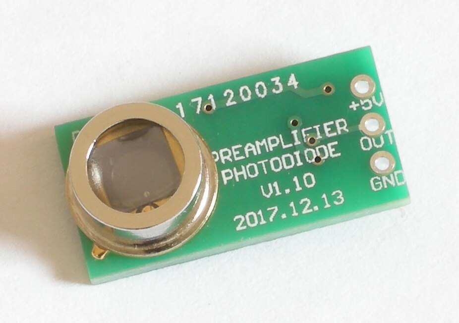
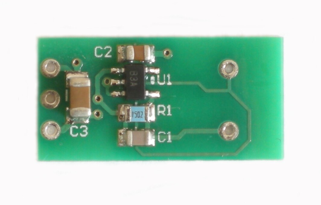
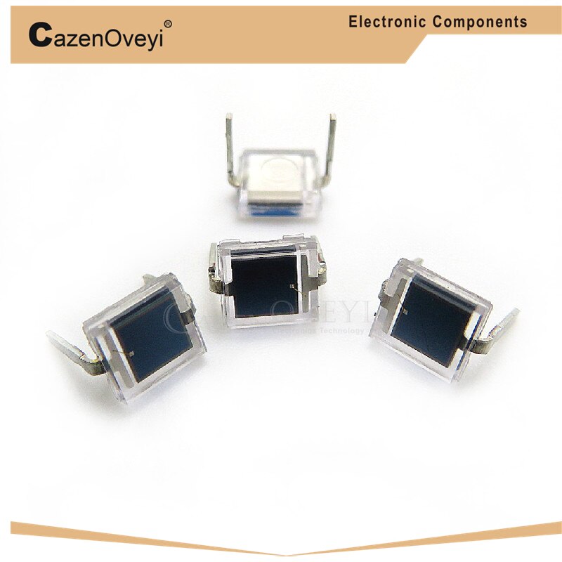
Photodiode Amplifier Module Light Intensity Detection Module Illuminance Meter
Photodiode is one of the most commonly used sensor types in many optical measurements。Such as absorption and emission spectra、Color measurement、Turbidity、Gas detection and other applications rely on photodiodes to achieve precise optical measurement。The photodiode generates a current proportional to the amount of light that hits the active area。Most measurement applications require transimpedance amplifiers,In order to convert the photodiode current to the output voltage。chart1Schematic diagram of display circuit。
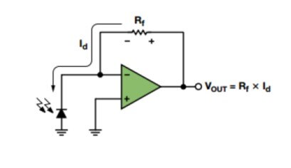
chart1 Simple transimpedance amplifier circuit
The photodiode of the circuit works in photovoltaic mode,The operational amplifier keeps the voltage on the photodiode at 00 V。This is the most common configuration in precision applications。The voltage current curve of photodiode is very similar to that of conventional diode,But the whole curve of the former will move up or down with the change of light level。chart2aDisplay the typical transfer function of photodiode。chart2bIs the enlarged figure of the transfer function,It shows that even in the absence of light,The photodiode also outputs a small amount of current。The dark current increases with the reverse voltage on the photodiode。Most manufacturers operate at a reverse voltage of 010 mVThe dark current of the photodiode is given on the premise of the calculation。
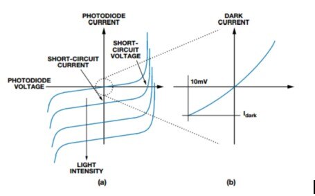
chart2 Typical photodiode transfer function
When the light reaches the active area of the photodiode,The current flows from the cathode to the anode。Ideally,All the photodiode current flows through the graph1The feedback resistance in the circuit,Produces a feedback voltage equal to the photodiode current times the feedback resistor。The circuit is simple in principle,However, if the system is to have the best performance, some problems must be solved。
DC considerations
The first problem is to select the operational amplifier whose DC specifications match the application requirements。For most applications,Low input offset voltage is the most important specification。There is an input offset voltage at the output of the amplifier,The offset voltage will increase the total system error;And in the photodiode amplifier,It also produces other errors。There is an input offset voltage on the photodiode,Generate more dark current,Further increase the system misalignment error。Calibration by software、AC coupling——Or both——Eliminating initial DC offset,However, large misalignment error will reduce the dynamic range of the system。Fortunately,,The input offset voltage is in the range of several hundredmVEven dozensmVWithin the scope of,There are many operational amplifiers to choose from。The second important DC specification is the input leakage current of the operational amplifier。The current enters the input of the operational amplifier,Or go anywhere other than the feedback resistor,Will produce measurement error。There is no operational amplifier with zero input bias current,But someCMOSorJFETThe input operational amplifier is very close to this value。FETThe input bias current of the input amplifier increases exponentially with increasing temperature。Many operational amplifiers are available85°Cor125°CSpecifications under;But if not,Then a better approximation isFor every ten degrees increase in temperature,The current doubles。
Another problem is to design circuits and lay them out,So as to minimize the external leakage current path——Leakage current will affect the performance of low input bias current operational amplifiers。The most common external leakage current path is the printed circuit board itself。for example,chart3Display chart1A feasible layout of photodiode amplifier。The pink line indicates that+5 VPower supply rail,Power the amplifier and deliver power to the rest of the circuit board。If in+5 VThe resistance between the wiring and the wiring carrying the photodiode current is equal to5 G(chart3China and IsraelRLexpress),that1 nAThe current will flow from+5 VRouting into amplifier。obviously,This is related to careful selection in application1 pAThe operational amplifier’s target is in conflict with each other。One way to minimize the external leakage current path is to increase the resistance between the circuit carrying the photodiode current and any other circuit。This may be as convenient as adding a larger routing exclusion zone around the routing to increase the distance from other routing。In some extreme applications,Some engineers will cancel it at the same timePCBRouting,Expose the photodiode lead to air and connect it directly to the input pin of the operational amplifier。
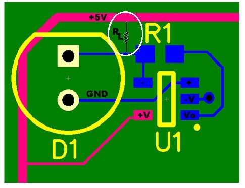
chart3 Photodiode layout with leakage current path
Another way to prevent external leakage current is to place a protective circuit beside the circuit carrying photodiode current,And make sure that both wires are driven to the same voltage。chart4Shows the protection routing around the network with photodiode current。+5 VThe leakage current generated by the wiring then passes throughRLInflow protection routing,Instead of flowing into the amplifier。In this circuit,The voltage difference between the protection line and the input line is only related to the input offset voltage of the operational amplifier——This is another reason why a low input offset voltage amplifier is used。
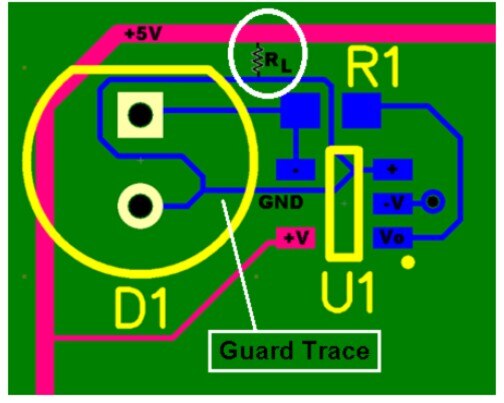
chart4 Using protective wiring to reduce external leakage current
‘
Reviews
There are no reviews yet.