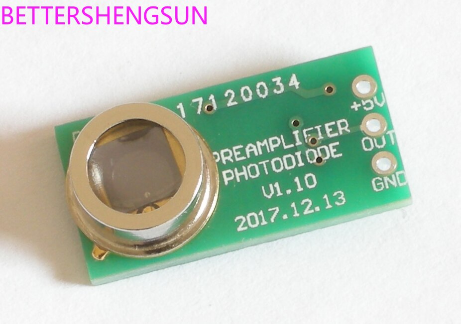
Description
- Origin: CN(Origin)
- Sensor Type: Holzer
Photodiode is one of the most commonly used sensor types in many optical measurements. Applications such as absorption and emission spectrum, color measurement, turbidity and gas detection all depend on photodiode to realize precise optical measurement. Photodiode generates a current proportional to the amount of light emitted to the active area. In most measurement applications, cross-resistance amplifiers are required to convert photodiode current into output voltage.Figure1Schematic diagram of the display circuit.
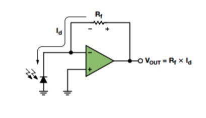
Figure1 Simple trans-resistance amplifier circuit
The photodiode of the circuit operates in photovoltaic mode, where the operational amplifier maintains the voltage on the photodiode0 V. This is the most common configuration in precision applications. The voltage-current relationship curve of photodiode is very similar to that of conventional diodes, but the whole curve of the former will shift upward or downward with the change of illumination level. Figure2aDisplays typical photodiode transfer functions. Figure2bIt is an enlarged graph of the transfer function, indicating that even in the absence of light, photodiode will output a small amount of current. This dark current will rise with the increase of photodiode on the backward voltage. Most manufacturers in backward voltage10 mVThe dark current of photodiode is given.
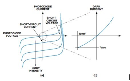
Figure2 Typical photodiode transfer function
After the light reaches the active area of photodiode, the current flows from the cathode to the anode. Ideally, all photodiode of the current flows through the graph.1The feedback resistor in, which generates a value equal to photodiode current multiplied by the feedback voltage of the feedback resistor. The circuit is very simple in principle, but some problems must be solved if the system has the best performance.
DC considerations
The first problem is to select the operational amplifier whose DC specifications match the application requirements. For most applications, low input offset voltage is the most important specification. There is an input offset voltage at the output of the amplifier, which will increase the total error of the system. In photodiode amplifier, it will also produce other errors. The input offset voltage exists on photodiode, which generates more dark current and further increases the system offset error. Through software calibration and AC coupling—Or both—Eliminate the initial DC offset, but larger offset error will narrow the dynamic range of the system. Fortunately, the input offset voltage is several hundredmVEven dozensmVThere are a large number of operational amplifiers to choose from. The second important DC specification is the input leakage current of the operational amplifier. The current enters the input terminal of the operational amplifier or anywhere other than the feedback resistor, which will cause measurement errors. Operational amplifiers with zero input bias current do not exist, but someCMOSOrJFETThe input operational amplifier is very close to this value.FETThe input bias current of the input amplifier increases exponentially with the increase of temperature. Many operational amplifiers provide85°COr125°CThe following specifications; However, if not provided, a better approximation isThe current doubles for every ten degrees of temperature rise..
Another problem is to design and layout the circuit to minimize the external leakage current path.—Leakage current will affect the performance of low input bias current operational amplifier. The most commonly used external leakage current path is the printed circuit board itself. For example, a graph3Display chart1A feasible layout of medium photoelectric diode amplifier. Pink routing indicates+5 VThe power supply rail supplies power to the amplifier and delivers power to the rest of the circuit board. If in+5 VThe resistance between the routing and the routing with photodiode current is equal5 G(Figure3ZhongzhongRLRepresentation), then1 nAThe current will be from+5 VThe trace flows into the amplifier. Obviously, this is related to careful selection in the application.1 pAThe target of the operational amplifier is contrary. One way to minimize the external leakage current path is to increase the resistance between the traces carrying photodiode current and any other traces. This may be as convenient as adding a larger route forbidden zone around the route to increase the distance from other routes. In some extreme applications, some engineers cancelPCBLine the photodiode lead exposed to the air and directly connected to the input pin of the operational amplifier.
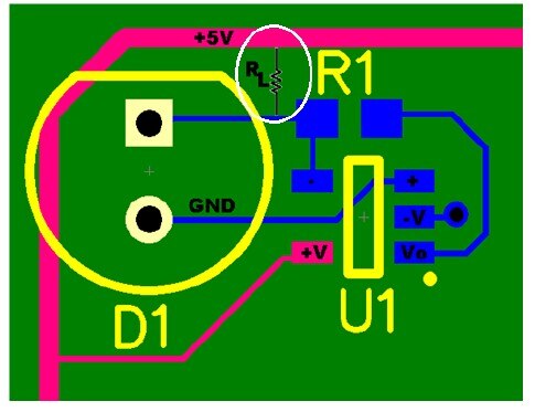
Figure3 Photodiode layout with leakage current path
Another way to prevent external leakage current is to lay out a protective trace beside the trace carrying photodiode current, and ensure that both traces are driven to the same voltage. Figure4Displays the protection traces around the network with photodiode current.+5 VLeakage current generated by routing then passes throughRLInflow protection traces, not inflow amplifiers. In this circuit, the differential pressure between the protection trace and the input trace is only related to the input offset voltage of the operational amplifier.—This is another reason why low input offset voltage amplifier should be selected.
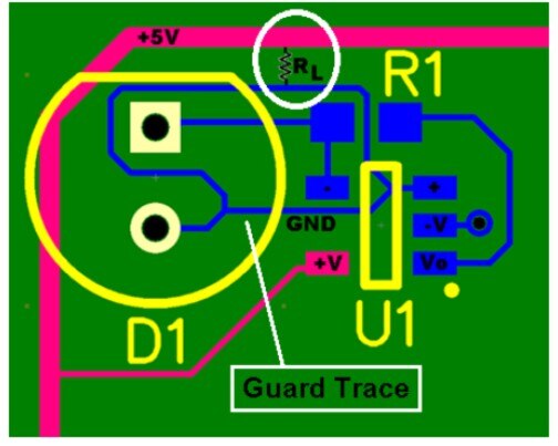
Figure4 Use protective traces to reduce external leakage current
Reviews
There are no reviews yet.