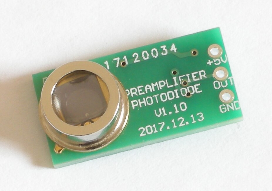
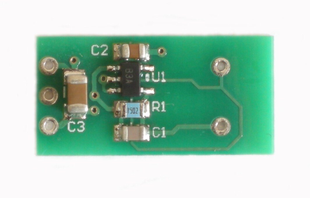
Description
- DIY Supplies: ELECTRICAL
- Certification: DOT
- Origin: CN(Origin)
Photodiode is one of the most commonly used sensor types in many optical measurements。Such as absorption and emission spectra、Color measurement、Turbidity、Applications such as gas detection depend on photodiodes to achieve precision optical measurement。The photodiode generates a current proportional to the amount of light irradiated into the active area。Transimpedance amplifiers are required for most measurement applications,To convert the photodiode current into an output voltage。chart1Schematic diagram of display circuit。
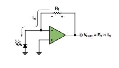
chart1 Simple transimpedance amplifier circuit
The photodiode of the circuit works in photovoltaic mode,The operational amplifier keeps the voltage on the photodiode at0 V。This is the most common configuration in precision applications。The relationship between voltage and current of photodiode is very similar to that of conventional diode,However, the whole curve of the former will translate upward or downward with the change of illumination level。chart2aTypical photodiode transfer functions are shown。chart2bIs the enlarged graph of the transfer function,Shows that even in the absence of light,Photodiodes also output a small amount of current。This dark current will rise as the reverse voltage on the photodiode increases。Most manufacturers operate at a reverse voltage of10 mVThe dark current of photodiode is given。
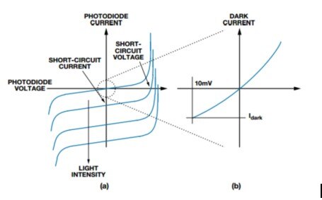
chart2 Typical photodiode transfer function
After the light irradiates the active area of the photodiode,Current flows from the cathode to the anode。Ideally,All photodiode currents flow through the figure1Feedback resistance in,A feedback voltage with a value equal to the photodiode current multiplied by the feedback resistance is generated。The circuit is simple in principle,However, some problems must be solved if the system is to have the best performance。
DC considerations
The first problem is to choose an operational amplifier with DC specifications that match the requirements of the application。For most applications,Low input offset voltage is the most important specification。There is an input offset voltage at the amplifier output,This offset voltage increases the total system error;In the photodiode amplifier,It also produces other errors。There is an input offset voltage on the photodiode,Generate more dark current,Further increase the system offset error。Calibration by software、AC coupling——Or both——Eliminate initial DC offset,However, large misalignment error will reduce the dynamic range of the system。Fortunately,,The input offset voltage is in the hundredsmVEven dozensmVWithin the scope of,There are a large number of operational amplifiers to choose from。The second important DC specification is the input leakage current of the operational amplifier。The current enters the input of the operational amplifier,Or enter anywhere other than the feedback resistance,Will produce measurement errors。Operational amplifiers with zero input bias current do not exist,But someCMOSorJFETThe input operational amplifier is very close to this value。FETThe input bias current of the input amplifier increases exponentially with the increase of temperature。Many operational amplifiers are available85°Cor125°CSpecifications under;But if not provided,Then a better approximation isEvery ten degrees of temperature rise,The current doubles。
Another problem is to design the circuit and layout it,This minimizes the external leakage current path——Leakage current will affect the performance of low input bias current operational amplifier。The most common external leakage current path is the printed circuit board itself。for example,chart3Display diagram1A feasible layout of photodiode amplifier in。Pink lines indicate+5 VPower rail,Power the amplifier and deliver power to the rest of the circuit board。If in+5 VThe resistance between the wiring and the wiring carrying the photodiode current is equal to5 G(chart3ZhongyiRLexpress),that1 nAThe current will flow from+5 VRouting into amplifier。obviously,This is related to careful selection in application1 pAThe objective of the operational amplifier is violated。One way to minimize the external leakage current path is to increase the resistance between the routing carrying the photodiode current and any other routing。This may be as convenient as adding a large routing exclusion zone around the route to increase the distance from other routes。In some extreme applications,Some engineers will cancel it togetherPCBRouting,Expose the photodiode lead to air and connect it directly to the input pin of the operational amplifier。
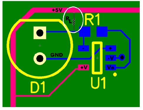
chart3 Photodiode layout with leakage current path
Another way to prevent external leakage current is to arrange a protective wiring next to the wiring carrying photodiode current,And ensure that both wires are driven to the same voltage。chart4Displays the protection routing around the network carrying the photodiode current。+5 VThe leakage current generated by routing is then passed throughRLInflow protection routing,Instead of flowing into the amplifier。In this circuit,The voltage difference between the protection line and the input line is only related to the input offset voltage of the operational amplifier——This is another reason why we choose low input offset voltage amplifier。
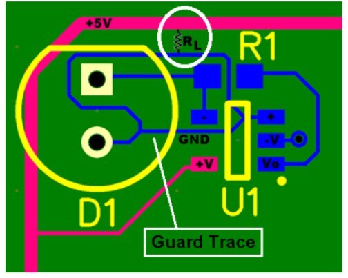
chart4 Using protective wiring to reduce external leakage current
Reviews
There are no reviews yet.