Description
Photodiodes are one of the most commonly used sensor types in many optical measurements. Applications such as absorption and emission spectroscopy, color measurement, turbidity, gas detection, etc. rely on photodiodes for precision optical measurements. The photodiode produces a current that is proportional to the amount of light that is incident on the active area. Transimpedance amplifiers are required for most measurement applications to convert photodiode current to output voltage. Figure 1 shows a schematic diagram of the circuit.
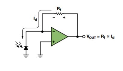
Figure 1 Simple transimpedance amplifier circuit
The photodiode of this circuit operates in photovoltaic mode where the op amp maintains a voltage of 0 V across the photodiode. This is the most common configuration for precision applications. The voltage-current curve of a photodiode is very similar to a conventional diode, but the entire curve of the former shifts up or down as the light level changes. Figure 2a shows a typical photodiode transfer function. Figure 2b is an enlarged graph of the transfer function, showing that the photodiode outputs a small amount of current even in the absence of light. This dark current rises as the reverse voltage on the photodiode increases. Most manufacturers give the dark current of the photodiode with a reverse voltage of 10 mV.
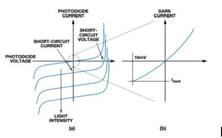
Figure 2 Typical photodiode transfer function
After the light is irradiated onto the active area of the photodiode, current flows from the cathode to the anode. Ideally, all photodiode currents flow through the feedback resistor in Figure 1, producing a feedback voltage equal to the photodiode current multiplied by the feedback resistor. The circuit is simple in principle, but some problems must be solved if the system has the best performance.
DC considerations
The first challenge is to choose an op amp that meets the requirements of the DC specification application. For most applications, low input offset voltage is the most important specification. There is an input offset voltage at the output of the amplifier, which increases the total system error; in photodiode amplifiers, it also produces other errors. There is an input offset voltage on the photodiode that produces more dark current, further increasing the system offset error. The initial DC offset is eliminated by software calibration, AC coupling, or both, but larger offset errors reduce the system dynamic range. Fortunately, the input offset voltage is in the range of a few hundred mV or even tens of mV, and a large number of operational amplifiers are available. The second most important DC specification is the input leakage current of the op amp. Measurement errors occur when current enters the op amp input or enters anywhere other than the feedback resistor. An op amp with zero input bias current is not present, but some CMOS or JFET input op amps are very close to this value. The input bias current of the FET input amplifier rises exponentially with increasing temperature. Many op amps are available at 85°C or 125°C; but if not provided, a good approximation is that for every ten degrees of temperature rise, the current doubles.
Another challenge is to design the circuit and layout it to minimize the external leakage current path—leakage current can affect the performance of low input bias current op amps. The most common external leakage current path is the printed circuit board itself. For example, Figure 3 shows one possible layout of the photodiode amplifier of Figure 1. The pink trace indicates the +5 V rail that powers the amplifier and delivers power to the rest of the board. If the resistance between the +5 V trace and the trace carrying the photodiode current is equal to 5 G (indicated by RL in Figure 3), then 1 nA will flow from the +5 V trace to the amplifier. Obviously, this is contrary to the goal of carefully selecting a 1 pA op amp in the application. One way to minimize the external leakage current path is to increase the resistance between the traces carrying the photodiode current and any other traces. This may be as convenient as adding a large routing exclusion zone around the trace to increase the distance from other traces. In some extreme applications, some engineers will cancel the PCB traces, expose the photodiode leads to the air and connect directly to the op amp input pins.
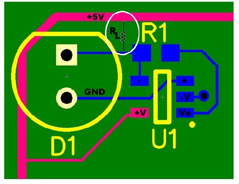
Figure 3 Photodiode layout with leakage current path
Another way to prevent external leakage current is to place a guard trace next to the trace carrying the photodiode current and ensure that both traces are driven to the same voltage. Figure 4 shows the protection traces around the network carrying the photodiode current. The leakage current generated by the +5 V trace then flows through the RL into the protection trace instead of flowing into the amplifier. In this circuit, the voltage difference between the protection trace and the input trace is only related to the op amp’s input offset voltage – which is another reason why a low input offset voltage amplifier is chosen.
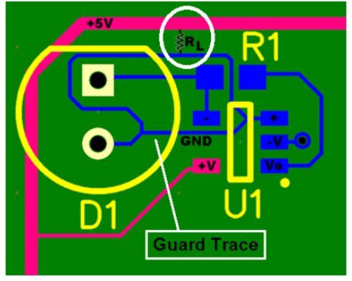
Figure 4 Using protective traces to reduce external leakage current
‘
Reviews
There are no reviews yet.